This failed standard LCD1602 dot matrix module will serve us as a perfect example of relatively advanced technology around us, which serves for years so well that we already stopped noticing how complicated these little things may be. The module consists basically of the LCD "glass" itself, a backlight, and the driver electronics. Now let's have a look also at the details.
Everybody knows, how such a module looks from the front, where it "shows" the two lines of characters, so let's first look at the backside. There's a PCB serving as a base there, with two ICs under the black epoxy "blobs" (one of the "blobs" on the picture has marks from being scraped with a knife, in a futile attempt to expose the silicon chip itself). This is a fairly standard way of doing these things, the chips being bonded directly to the PCB and then covered by the standard epoxy, rather than using regular packaged ICs - manufacturers of these modules make their best to save each and every penny. The chips here are "clones" of the de-facto industry standard Hitachi HD44780 and its companion chip. Quite a lot of manufacturers makes these on the far East. The "main" chip is in fact a controller, receiving commands and data through the system connector CON1, storing them, and periodically producing a sequence of signals to refresh the "image" on the display, in a time-multiplexing fashion. As it does not have enough "pins" to drive all the lines and columns of a 2-line 16-character display (i.e. 2x8=16 rows and 16x5=80 columns), a companion chip "expanding" the number of output "pins" is under the second "blob", effectively being just a serial-in-parallel-out shift register, periodically "filled" from the "main" controller.
The "system" connector - CON1 - is connected according a de-facto standard, too. There are two styles of this connector, either a single 14-pin row along the longer edge of the module - as is in this case, or a 2x7 pin row along the shorter edge of the module. Taking into account the standard way of numbering of two-row headers, the pinout is both styles is identical; but beware, there are a few "deviant" modules around, which have GND and VCC (pins 1 and 2) swapped, compared to the "more common standard". Always check the datasheet first.
The reader has certainly noticed that the module on picture has a 16-pin header, although 14-pin header is mentioned above as standard. The extra 2 pins are here dedicated to backlight supply. This is a fairly common arrangement, but beware: there is no guarantee as per the polarity, voltage, need of current limiting resistor etc. - although many modules have simply two LEDs in series, again, for safety, consult the datasheet. The backlight pins may also be located differently: on the "other side" before pin 1, with a gap from the "system" connector, or completely elsewhere (or the module may have no backlight at all, of course ;-) )

Traditionally, the PCB is layed out with a couple of options in mind. One of the main parameters is the supply voltage. While the integrated circuits are made in CMOS technology and are perfectly capable of running both with 5V and 3V supply voltage (with a minor change in the oscillator circuit, where resistor denoted RC is recommended to be changed for a slightly different value - see the IC's datasheet), the LCD itself requires a bias voltage of about 4.0-4.5V against the positive voltage rail. When operating at 5V, this voltage (around 0.5-1V against GND) is usually generated by a voltage divider (a potentiometer or trimmer) from VCC and fed to pin 3 of the connector. But, when operating at 3V, this voltage needs to be negative in respect to GND. It can be produced off-board and then connected to pin 3, as usual; but that would be naughty of the module manufacturer to push the user to do that ;-) . There is an area on the right-hand side of PCB, where an inverter based on the venerable Intersil ICL7660 charge-pump, or some of its maybe more than a dozen of clones produced worldwide, can be mounted (U3). A voltage divider (R8|RM + R10, vs. R7) and a transistor (Q1) can be provided to adjust the negative voltage to the exact value needed for optimal contrast; it is then connected to the LCD bias "ladder" (resistors R1-R5) through resistor R9 (while omitting resistor R6). Alternatively, the negative voltage from inverter can be directed outside the module by shorting jumper JV, through pin 15 (which is then obviously not used for backlight supply). The intention is to place a voltage divider (potentiometer) between this voltage and ground, and then feed back the adjusted voltage through pin 3.
The HD44780-compatible LCD controller allows to operate in a different mode, with 11 lines per character rather than 8. This involves a different, 11-step multiplex and requires a slightly different connection of the voltage divider "ladder", with resistor R3 being not a 0 ohm jumper. To allow for both modes with a the same values of all resistors, R3 can be jumpered through by shorting J3. However, as 11-line LCDs are rare, this option is not likely to be used.
There is also a jumper JD, to short the metal frame (more precisely, the pads where the frame holds the PCB), to the logic ground. This is a good thing to do, to avoid electroctatic charge from somebody touching the frame to find its way randomly through other, possibly more sensitive, paths.
As mentioned, there are several possible methods for powering the backlight, and there are also several options for the physical appearance of backlight itself. There are three pairs of holes marked A and K on the left-hand side of PCB, and two pairs on the other side, all connected together - indicating the five possible arrangement of the backlight system pins. There are also options for supplying the backlight: jumpers JA and JK, here both shorted by a drop of solder, connect the respective electrodes to pins 15 and 16 of CON1. As an alternative, shorting J1 and J2 would connect the respective backlight electrodes to pins 1 and 2, i.e. to the supply pins of the display's logic, eliminating the need for the two extra pins in the connector (or, two conductors in the cable leading to the module). Current to the backlight is limited by resistor RL, which is here a 0 ohm jumper; which means, that current limiting has to be provided by the outside circuit.

The backlight itself is positioned between the LCD "glass" (B) and the PCB (G). It consists of the LED diodes mounted on a miniature PCB (D), emitting to the edge of the lightguide; the lightguide (E) - a piece of acrylic plate; reflector below the lightguide (F) - a piece of glossy white paper; and a diffuser (C) - a piece of milky-white plastic film just above the lightguide. This whole assembly is then held down by the metal frame (A) to the PCB (G).
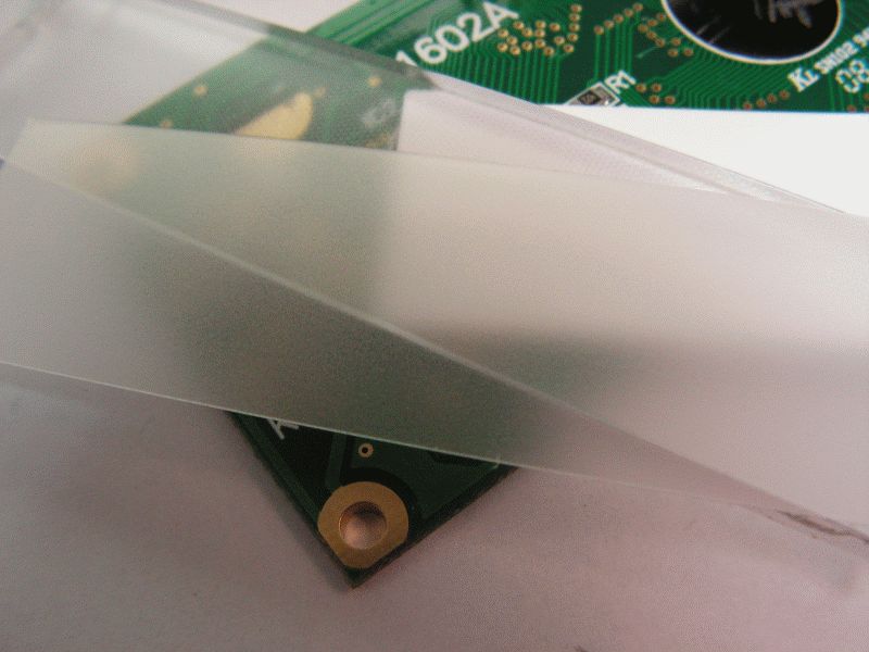
The lightguide is a remarkable piece of engineering in itself, providing an uniformly lit surface from two basically point-like sources of light. Yet it is ingeniously simple - it is simply a piece of acrylic plate, with LEDs shining into one of its short edge. One of its surfaces is covered by bumps. They are designed so that they reflect the light rays impinging in a rather shallow angle from inside the waveguide sharply to the other surface, where they don't reflect anymore, but come straight outside. Those rays which get through the bumps, are reflected back by the bottom reflector (the glossy white piece of paper). Three of the edges - except the one through which the LEDs light comes inside - are covered by a thin metal (presumably aluminium) foil to prevent the light to escape.
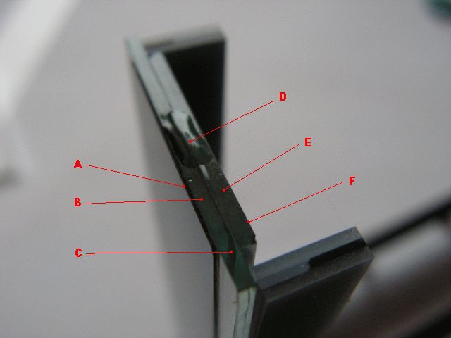
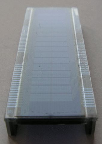
Finally, the most important constituent, the LCD "glass" itself. Again, a simple thing at the first sight. But it is a complex assembly again: two glasses ((B) and (E)), only a fraction of milimeter apart, separated by a spacer at the edges (shadow of which is seen as (C)), providing also a "container" for the liquid crystal itself (which is filled into that gap through a hole in the spacer, sealed by (D)). The "optical" function of LCD requires also to add two polarisers on bottom and top of the stack ((A) and (F)).
There is a set of semi-transparent electrodes in the shape of lines formed on each "glass", perpendicular to each other, forming a "mesh". At the intersection of the lines, electric field from voltage applied between the electrodes makes the liquid crystal's "crystals" to twist, turning polarisation of the light passign through, which is then absorbed at the respective polariser, making that square spot appear dark. The electrodes must pass most of the light through, though, and being conductive at the same time. The material of choice for such electrodes is so called ITO (indium-tin oxide), in a thin vacuum-deposited layer on the glass; and then, after a photolitographic step, selectively etched away to form the "lines", much as traces on PCBs are made. They are transparent when viewed "normally", but get visible when viewed at an angle.
The electrodes are brought out to the edge of the glass, where they form contacts on the bottom side of the top glass. The electrodes from the (top of) bottom glass - which form the "rows" - are "bridged" through the separator to similar "blind" contacts on the top glass, so both rows and columns contacts can lay on the same plane.
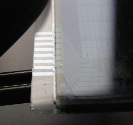
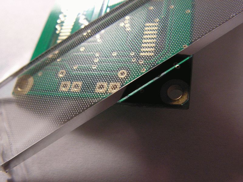
Finally, the contacts are connected to the respective pads on the PCB. To achieve that - and to allow for a space between the PCB and the glass where the backlight assembly will fit, the contacts are connected to the pads through a couple of rubber strips. Those are just one more example of simple yet effective technology: they consist of many very thin conductive stripes, stacked next to each other, but not touching each other, embedded inside non-conductive rubber. Note, that the stripes are much thinner than the width of the contacts - and, maybe more notably, thinner than the width of gap between contacts. Thus, given the pads on PCB are of the same shape and span than the contacts on the glass, there is no need for any special alignment, except the glass has to be positioned directly above the PCB with an error of maybe a millimeter - and the metal frame holding the whole assembly together easily ensures that.

Isn't it surprising, how much of remarkable technology is hidden even in such a simple, cheap and ubiquitous electronic part, as an alphanumeric LCD module is...
24/11/2009, wek at efton dot sk